A development board is an essential tool when working with projects that involve a microcontroller and most of the time you will also need a breadboard and a power supply. So why not combining all these in a single product?
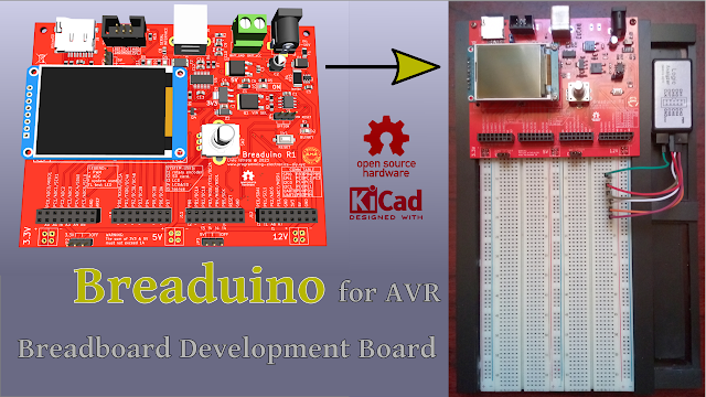
Meet Breaduino - a custom development board build around ATmega328PB microcontroller. If you are a beginner in electronics or microcontrollers, building a development board is not only rewarding but also educational.
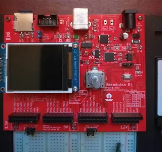
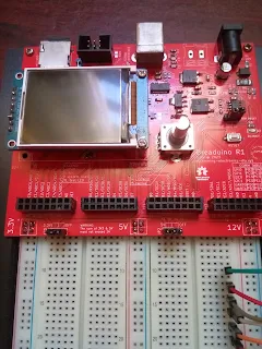
The Breaduino dev board is designed to be used with two breadboards where it outputs three voltages: 12V, 5V and 3.3V. It includes a TFT display, micro SD card socket, input current measurement and a rotary encoder for user interaction. On the right side of the case is space for a small logic analyzer and/or a 9V battery. All these are optional modules. Even the breadboard is optional so the board can be used standalone. Since this is a customizable board it can be modified to fit your needs.
Contents
- Schematics
- Construction Overview
- The Case
- Burning the bootloader
- Final thoughts
- Links
Schematics
The schematic is divided in three parts: power supply, USB interface and the microcontroller with it's modules. Let's first examine the power supply section.
The Power Supply
|
|
click to enlarge |
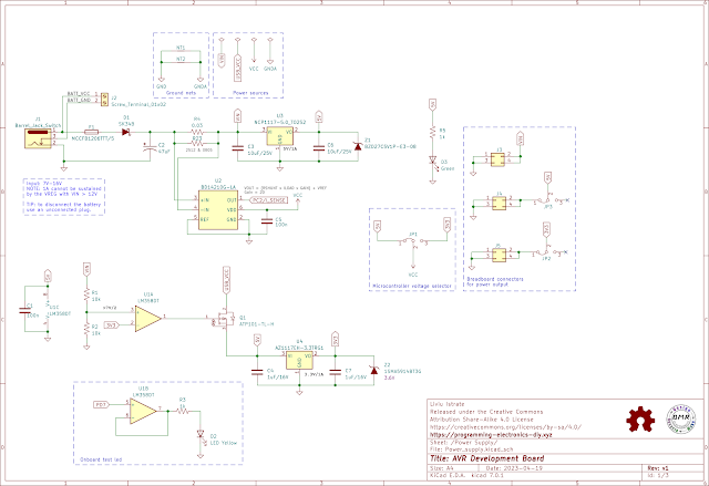
The board can be powered from 3 power supply sources: the power barrel jack, the battery screw header or the USB. Minimum input voltage is 7V and the maximum input voltage is around 16-20V. The maximum voltage depends on the 5V regulator although I don't recommend going over 12V since that will make the 5V regulator very hot even at relatively low currents of 200mA.
Screw terminal: for portability, a battery between 7V and 12V can be connected to the screw terminal.
DC barrel jack: this connector has 3 pins. The third pin is used to switch the ground from the battery so when a jack is inserted, the battery ground will be disconnected thus allowing only the power from the barrel connector in.
Fuse F1 and Zener diodes Z1 and Z2: this fuse is here to disconnect the input power in case there is a short circuit anywhere on the board or breadboard. This is especially important when using a battery that might not have a over-current protection like a DC wall adapter has. The fuse in the schematic is rated at 5A but I think that is too much. A 2 or 3A fuse would be better. You might think why not use a resettable poly-fuse? That might save you the trouble of replacing the fuse in case it blows. The reason is the zener diodes.
First what is their purpose there if the voltage regulators already output a steady voltage? Well, from my experience and online research I found that a voltage regulator can fail due to overheating and aging and let the input voltage go through them unimpeded. That will burn almost all components on the board and whatever you have connected on the breadboard that run on 5V and 3.3V. That would be more expensive than a Zener diode. To protect against that without expensive circuitry the idea is that when 12V is applied across Z1, the voltage will be clamped to 5V. The problem is that the power dissipation will be in the order of watts and high power zener are expensive and very bulky and so a smaller diode will burn out quickly. If the diode fails open-circuit than the over-voltage protection also fails. If the diode fails short-circuit than it is good since the PCB traces should handle the current until the fuse blows. Even smaller Zener diodes can handle peak currents of few amps for a few milliseconds so the idea is that the fuse would blow before the Zener fails but if the fuse is a resettable one then the Zener will eventually overheat and fail.
Diode D1: is a Schottky diode for reverse polarity protection especially needed when connecting the battery wires to the screw terminal. Easy to swap them and ruin your board. A Schottky type is used since it has a low voltage drop.
Input bulk electrolytic capacitor C2: a bulk capacitor is used to prevent the output voltage of a supply from dropping too far during the periods when current is not available. Because the wires have inductance, the current can not increase instantly when a consumer needs it so a capacitor acts as a current reservoir. The higher the current draw the larger the capacitor should be. Here is not needed a very large capacitor since through-hole capacitors can be placed across the breadboard power rails if needed.
5V linear voltage regulator: this regulator is rated for 1A and also powers the 3.3V regulator so make sure that the total current draw from 5V and 3.3V does not exceed 1A. C3 and C6 are 10uF input and output ceramic capacitors with the size being selected according to the datasheet. Ceramic or tantalum capacitors are used since they have a lower ESR (Equivalent Series Resistance) and can handle the peak currents better than the electrolytic ones. The maximum voltage drop is 1.2V so the input voltage should be at least 5V + 1.2V.
The thermal pad should be connected to a largest copper area as possible on top and bottom layers using a few via (6 should be enough).
3.3V linear voltage regulator: the power source for this one can be either the output from the 5V regulator or the USB. The rated current is 1A since it has to power the display, the SD card and the 3.3V breadboard rail.
Power ON led indicator: led diode D3 and R5 are used to indicate that 5V is present. I use an 0805 green led for this purpose. The resistor is sized to limit the current to less than 1mA since it's an indicator led not a flashlight.
Microcontroller voltage selector: JP1 is a 3 pin header jumper used to select the voltage for microcontroller: 3.3V or 5V. This is useful when interfacing with 3.3V devices. With a simple jumper you can avoid using voltage level shifting. But care must be taken since if you select 5V when you wanted 3.3V, there is no protection against that. Why not wire it at 3.3V permanently then? Well, the datasheet does not guarantee reliable functionality when the microcontroller is powered from less than 4 volts and the CPU is clocked at 16MHz. It works with 3.3V and 16MHz crystal but i guess there could be scenarios when something could go wrong. But for a dev board this is not an issue. Apart from that you might have 5V only devices that you want to interface with the MCU and then you will need a voltage translator.
Breadboard output power connectors: J3, J4, J5 are 2 pins and 2 rows
pin header connectors with 2.54mm pitch used to output 12V, 5V and 3.3V to the
breadboard rails. Two or three pins are recommended to lower the contact
resistance and thus minimize the voltage drop. These are the only parts
mounted under the board. JP3 and JP2 are 3 pin jumpers used to switch off the
5V and 3.3V rails.
Input voltage selector: the op-amp LM358DT (U1) switches between 5V
from USB and 5V from the voltage regulator. Because the USB voltage could be
less than 5V, connecting these nets together could push current to the USB due
to voltage difference, which is not a good thing. The P-Channel mosfet Q1 is
used to isolate the two sources. The ATP101-TL-H was the only P-Channel mosfet
I had. It can handle 25A which is ridiculously high for this application, but
you can replace it with a smaller one since it can only has to handle the
current from USB which is maximum 500mA.
Let's see how the op-amp will select the power supply in each case scenario. Here VIN means the power from the DC barrel or the battery connected to the screw terminal and USB_VCC represents the power from USB.
- VIN on, USB_VCC off: when VIN is present the 5V will be generated which in turn produces the 3.3V that is connected to the (-) pin of the op-amp. VIN is divided in half by R1 and R2 so if VIN is 12V, the voltage on the (+) pin will be 6V. Since the voltage on the (+) pin is higher than on the (-) pin, the op-amp will output high turning off the mosfet.
- VIN off, USB_VCC on: if USB power is present and VIN is off, the 5V from USB will go through the mosfet's diode to the 5V rail generating 3.3V. Now the (-) op-amp pin will be at 3.3V and the (+) will be pulled to ground by R2. Since (-) is higher than (+) in voltage the op-amp will output low turning on the mosfet lowering the voltage drop across the mosfet. Something to be aware of here is that the 5V from USB will go back through the output of the 5V regulator to the input and so VIN will be 5V minus a diode voltage drop that is inside the regulator. This is not an issue since this circuit is used by Arduino and it is proven to be working.
- VIN on, USB_VCC on: when both power sources are on the 5V and 3.3V
will be generated by VIN since the USB voltage is not greater than 5V
(hopefully) so the mosfet body diode will not conduct. Again, on (-) pin we
have 3.3V and on the (+) pin is VIN / 2. Any voltage on VIN greater than 7
will make the (+) pin higher than (-) making the op-amp output a high level
thus turning off the mosfet which will isolate the USB supply leaving VIN
active.
The onboard test led: since LM358 is a dual op-amp the other comparator is used to buffer a pin from the microcontroller and control a led. Connecting the led directly to a pin could affect the pin functionality when used with something else but since the input of the op-amp takes almost no current, the pin can be used for other purposes regardless if you want to blink the led. Having an onboard led is very useful when debugging code - just set the state of the led somewhere in the code and you can find if and where the code is stuck in a loop, see what if/else statements gets executed, or blink it with 1 second delay to test if the CPU is clocked at the frequency that you think it is.
The port pin for the onboard test led is PD7 based on some criteria like: must not be an ADC or PWM pin, must not be used by the display, SD card or rotary encoder. On first prototype, I've made the mistake of using the SCK pin like Arduino does but when SPI is enabled, such as when using the display or the SD card, the state of SCK pin cannot be changed making the led unusable. Also the led was not lighting up during SPI communication because one, the op-amp is too slow for that and second the pulses on SCK are too short for the led to emit any visible light.
Current Sensing
In many projects I needed to know how much current a motor or a module consumes and using a multimeter is just a hassle. So I've decided to add a circuit that could measure the input current. In case you don't need this feature you can exclude it.
There are many methods to measure current. Almost all of them requires a current sense resistor. In the schematic they are R4 and R23. Only one resistor is needed. The reason there are two is to have placeholders for two different sizes: 2512 and 0805. You can use one of them depending on the maximum current you want to measure and what resistors you have.
In the first prototype I naively thought that I could get away by using one voltage divider on each side of the resistor and measure the voltage using the ADC. I didn't expect much precision but when I tried to measure it, the current varied few hundred milliamps. After making a spreadsheet and playing with values I realized this won't work. I won't go in details since it would take too much explanations.
There are two methods of current sensing called high-side and low-side. Low-side current measurement is when the sense resistor is placed between the load and ground. It is the easiest to measure with the disadvantage of affecting the ground potential of the load. In most cases that is not an issue, for example when charging a battery. High-side measuring is when the sense resistor is placed between the power supply and the load as in our case.
Another way would be to use an op-amp in a differential configuration. I had good results with this approach in other projects but the resistor was on the low-side. For the high-side, a rail-to-rail op-amp is needed but they are more expensive. The common op-amps such as LM321, LM324, LM358 won't work because of the common mode input voltage, meaning the voltage on input pins must not exceed usually VCC - 2V but in our case the op-amp supply voltage is the same as the measured voltage.
The best approach is to use a dedicated IC that is designed for measuring the current. Nowadays this is a more affordable solution. They already include laser trimmed precision resistors so they take less space on the PCB and are much more accurate than using discrete resistors.
The IC U2 is BD14210G-LA current sense amplifier. Can be powered from 2.7 to 5.5V but it can take up to 26V on it's inputs. In the past i have used INA types but this one is cheaper and also has a low gain of 20. Most INA that I could find had gains of 50, 100. You will see later when running the numbers how the gain affects the selection of current sense resistor, the reference voltage of the ADC. The chip is very easy to use requiring only a decoupling capacitor. The tricky part is to calculate the value of the sense resistor based on the minimum and maximum measured current and ADC reference voltage. At the end I will be linking a spreadsheet that will help in calculating the necessary parameters.

|
|
from BD14210G-LA datasheet |
In the above figure the reference pin is set at half the supply voltage. This is useful when measuring bi-directional currents but for our purpose this is not needed so the reference pin is grounded.
ADC reference voltage
Before calculating the value of current sense resistor, we have to decide what should be the reference voltage of the ADC. The ATmega328PB microcontroller has a 10-bit ADC and the reference voltage could be internal 1.1V, VCC or any voltage we apply on the AREF pin of the microcontroller. Using an external voltage would be better but that would mean extra cost and extra components. Using the VCC, which can be 5V or 3.3V depending on what voltage the micro is set to run on, would allow a higher voltage from the current sense IC but the ADC voltage step size will be around 5mV as opposed to 1mV if 1.1V is used.
A 10-bit ADC has 2^10 - 1 = 0 to 1023 ADC units. A value of 1023 represents the reference voltage. So a voltage measured by an ADC pin must not exceed the reference voltage. Assuming the ref voltage is 1.1V and on the ADC pin is applied 1.8V then the ADC will report maximum value 1023. Applying a voltage higher than the VCC will damage the microcontroller.
Calculating the ADC voltage step size based on reference voltage:
Vref / 1023
If Vref = 1.1 / 1023 = 0.001 = 1mV
If Vref = 5 / 1023 = 0.0048 = ~5mV minimum voltage resolution.
Calculating the ADC current step size:
Imin = ADCvstep / Rsense / Gain
Where:
ADCvstep is the voltage step size.
Rsense is the value of the sense resistor. Let's say 0.03 ohms.
Imin = 0.001V / 0.03 / 20 = 0.0017A (1.7mA)
To lower this value and improve current resolution we could use a chip with a
larger gain or a higher value resistor but that would output a higher voltage
than ADC vref could use, or use a 12-bit ADC to lower the ADCvstep but that is
way too much for our application.
Calculating the current sense resistor:
(Vref - Voffset) / (Imax * Gain)
Where:
Vref is the ADC reference voltage. Let's select 1.1V since it has a low 1mV
voltage resolution.
Voffset is the voltage reference of the current sense IC which in this case is 0.
Imax is the maximum current we need to measure. Say we want to measure maximum
1.8A.
Gain is the gain of the current amplifier IC which in this case is 20.
1.1V / (1.8 * 20) = 0.03 ohm resistor (30 milliohms)
Calculating the maximum resistor power dissipation at the rated current:
Imax^2 * Rsense
1.8^2 * 0.03 = 0.097W (97 milliwatts)
The smaller the resistor value is the less power it dissipates and so it can measure higher currents but the voltage drop across it will be smaller which can make it harder to measure accurately.
Calculating the voltage drop across the current sense resistor:
Vsense = Isense * Rsense
Assuming the maximum current Imax is 1.8A then 1.8 * 0.03 = 0.054V (54mV).
As previously calculated the minimum current Imin is 1.7mA then 0.0017 * 0.03 = 0.05mV (50uV).
Calculating the current sense amplifier output voltage:
Vout = (Rsense * Iload * Gain) + Vref
Since in our case the Vref is 0 it can be ignored.
At the maximum current Imax, Vout = 0.03ohms * 1.8A *20x = 1.08V which is well
below the 1.1V ADC reference.
At the minimum current Imin, Vout = 0.03ohms * 0.0017A *20x = 0.001V (1mV)
which fits in the calculated ADC voltage step size of 1mV when the ADC
reference voltage is 1.1V.
USB Interface

|
|
click to enlarge |
A useful feature to have in a development board is the ability to transfer data between the microcontroller and a PC. Having an USB interface allows us to power the board just by using the USB cable, easily program the microcontroller, to send data via UART back and forth that is also useful for debugging code and also we can plot data with it.
The IC used for USB interface is FT231XS made by the FTDI company. It's job is to convert between UART and USB protocols. I prefer this over FT232 because is cheaper and TX and RX pins are 5V tolerant meaning it doesn't need a voltage shifter.
This IC is connected to the UART 0 of the microcontroller through the RXD (Receive) and TXD (Transmit) pins. Any UART interface must have RX connected to TX and TX from microcontroller to RX on FTDI chip. D5 is a red led that indicates UART transmission and D4 is a yellow led that indicates reception.
Starting from the left we have a USB type B connector. Power from the USB goes through a PTC (Positive Thermal Coefficient) resettable fuse F2. This protects the USB host by limiting the current to 500mA. In case of a short circuit the fuse heats up increasing it's resistance thus limiting the current to very low value. When the short is removed the fuse cools down and it's resistance drops as well. That's why is called a resettable fuse.
The rest of the components are there to suppress and filter EMI noise. The ferrite bead FL2 stops high-frequency switching noise from the IC to be induced on the USB power supply. C11 and C12 are decoupling capacitors - they act as a current reservoir for the chip during peak current draw. The 10uF capacitor filters lower frequency whereas the 100nF filters higher frequency noise to ground. USB_VCC is the 5V supply for the IC and also powers the development board.
R6 and R7 are termination resistors placed at the end of the transmission line to prevent the signal from bouncing back thus ensuring signal integrity. They are encountered when high-speed transmission using differential pairs is involved.
RV1 and RV2 varistors are used to protect the IC from ESD spikes by conducting the energy to ground. Notice that the USB shield is connected to ground through FL1 ferrite bead. This ensures that any ESD voltage spike will be absorbed by the inductor and will not affect the ground potential.
The microcontroller and peripherals

|
|
click to enlarge or right click to open in a new tab |
Les's first examine the ATmega328PB microcontroller circuit. Starting from left, AREF pin is decoupled through 100nF capacitor as specified in the datasheet. This is only the case when no external voltage reference is applied to the ADC.
CPU clock
By default AVR microcontrollers are using the internal 8MHz clock generator but are actually running at 1MHz because the divide CPU clock by 8 fuse bit is set. We want a higher speed than that so a 16MHz crystal is used. If I remember the specs correctly the highest speed that the CPU can be safely clocked is 20MHz, but 16MHz is more commonly used I guess because it divides better when using delays and such and can also work better with 3.3V supply. The two capacitors (C15, C16) are there to help the crystal oscillate and their value could make the frequency lower or higher than nominal. Consult the crystal oscillator datasheet for the recommended value. The high value resistor R18 in parallel with the crystal, from what I understand, is a biasing resistor and it reduces the oscillation start-up time. For more information on this topic search for "Pierce crystal oscillator".
Reset pin
The reset pin is held high through a 10k pull-up resistor and connected to ground through a momentary tactile push button SW1. When the button is pressed the pin is connected to ground restarting the microcontroller. The rest of the reset circuit is used for programming the microcontroller via the USB.
DTR signal
The DTR signal is generated by the USB to serial converter IC and it is used
to reset the microcontroller before programming it.
How is the DTR pin used to program the microcontroller
DTR stands for Data Terminal Ready and is one of the control signal that belongs to RS-232 serial communication. In the context of programming a microcontroller we use this pin to reset the microcontroller (MCU). When you upload the code to the microcontroller, the host PC will pull this pin low, but having an MCU in a reset state is of no use. So to convert the low state to a low short pulse, we place a non-polarized capacitor C19 in series with the DTR signal. This low pulse will reset the microcontroller and if a bootloader is present, it will be loaded. Then the bootloader will take the code received from the PC and write it on the microcontroller.
DTR reset issue
In order to support both 3.3V and 5V microcontrollers, the FTDI is configured to output only 3.3V on I/O pins. When the microcontroller is powered from 3.3V there is no issue but when it uses 5V then the DTR which is at 3.3V will not be able to trigger the reset every time. This is an intermittent issue. The problem has to do with how the capacitors work. Initially one capacitor plate is charged at 5V through the pull-up reset resistor and the other side is charged at 3.3V by the DTR pin. When the DTR is pulled low, the reset side will not be at 0 volts but 1.7V instead (5 - 3.3 = 1.7V). This voltage is not low enough to have a reliable reset nor high enough to prevent the reset all the time. The reset will occur or not depending of electrical noise. For example when I was putting my finger on the reset line while programming or connect a logic analyzer, the reset would work.
When the DTR signal goes high again, the voltage on the reset node will
spike to 5 + 3.3 = 8.3V but this from what I understand is not a concern
since the Reset pin is the only pin able to withstand 12V without damage.
However a diode is placed in parallel with the pull-up reset resistor that
also helps in discharging the C19 reset capacitor.
Simple and cheap bi-directional voltage level shifter
To solve the DTR reset issue, a simple voltage level shifter can be implemented by using an N-channel mosfet and a 10k pull-up resistor Q4 and R19.
The DTR pin is connected to the source of the mosfet. Let's call this LV (low voltage) side. The mosfet drain is the DTR after has been voltage level shifted. Let's call this node HV (high voltage). When the DTR is driven low, the mosfet turns on pulling the HV low. When HV is driven low, LV is also driven low through the mosfet’s body diode, at which point the mosfet turns on. In all other cases, both LV and HV are pulled high to their respective logic supply voltages. The resistor (R19) on the HV side is required to pull-up the DTR to the voltage that the microcontroller runs at.
The N-channel mosfet can be of any type provided that the voltage gate threshold is below 3.3V. Recommended products are: NX7002AK, 2N7002PW.
The DTR disable jumper JP4 can be used to stop the PC to reset the microcontroller. Not sure when this could be an issue but it is better to have the option than not having it if you someday need it. I have noticed on Windows 10 that plugging/unplugging another USB device such a logic analyzer, was causing the microcontroller to reset. The same happen when opening a serial terminal.
AVCC is the analog power supply for analog circuitry inside the microcontroller such as the ADC and it is filtered by the inductor L1 and capacitor C21. Ideally this should be a steady noise free voltage for the ADC to perform as intended.
Microcontroller breakout headers
The 4 receptacle headers on the right are the main feature of a development board since there are all the necessary pins for... well... developing stuff. Each one is 2 rows by 8 pins. Having each output pin doubled has some benefits such as: you can use a logic analyzer on evey pin even if they are used in the project, if used without a breadboard there are two connections instead of one, decreasing contact resistance when using power from the headers by using two wires instead of one. If you can't find this type of connectors or they are more expensive, you could use two 1 row 8 pin headers. That's what I did. It's more difficult but it's doable. Tip: when cutting count 9 pins not 8 since near the cut the metal pin will sometimes fall off.
ICSP (In Circuit Serial Programming)
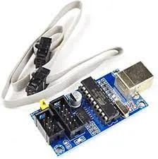
Header J7 it is used to upload the bootloader so the microcontroller can be programmed over the USB. It is using the SPI 0 interface module. This is also used to modify the fuses since that cannot be done over USB (UART). For this you will need an ISP programmer such as USBtinyISP or USBasp.
Be aware that the pins can be mirrored on some of these programmers so they could not match the header on the board. Check it first and if they don't match you can use jumper wires to connect each pin instead of the ribbon cable.
R15 is a placeholder for an 0805 0 ohm jumper resistor. If for some reason
you need to power the micro using the ISP programmer, solder a jumper
resistor there or use a blob of solder.
The TFT color display ST7735
This circuit is optional since the board can work without it but I think it is useful to have a display especially when you move the board around and there is no computer to output data using the UART. As with the DTR pin, here we are using again the same components for voltage level shifting - resistors R12 and R13 and mosfet Q2. The difference here is that there are two resistors not just one as before, R12 beeing used to speed up the rise time.
TFT reset pin: resistor R14 and small signal diode D6 are used to properly reset the display when the microcontroller is reset. This two components saves a precious microcontroller pin. At first i thought the pin can be tied to VCC and use software reset commands during diplay initialization but that did not work so I found this solution instead. The diode is used to protect the reset pin from 5V since the ST7735 is a 3.3V device.
The library code and other informations can be found here:
https://www.programming-electronics-diy.xyz/2022/02/library-for-st7735-tft-display-driver.html.
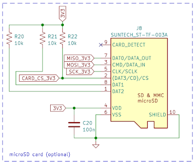
MicroSD memory card interface
The library code and other informations about the SD card interface can be found
at this link:
https://www.programming-electronics-diy.xyz/2022/07/sd-memory-card-library-for-avr.html.
One thing that I should mention here is the micro SD card socket. The one
that I've used is bought from eBay and has no brand so you might not have
the exact same type. Be sure to check the footprint dimmensions or print it
to scale before ordering the PCB.
Voltage Level Shifter
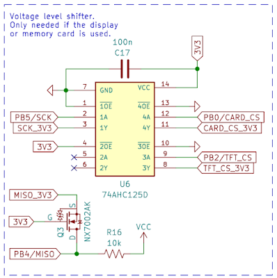
Since both the display and SD card are 3.3V devices and the microcontroller might run at 5V, we need to convert the 5V to 3.3V and vice-versa. The purpose of 74AHC125D is to do just that. The chip can translate 4 signals. The A pins are inputs and Y pins are the outputs. The output voltage is VCC which in this case is 3.3V. To enable the output, the specific OE (Output Enable) pin must be grounded, and to disable the output, the OE is connected to 3.3V.
The MISO pin is not used with this chip instead there is a discrete voltage level shifter. The reason is the display. Notice how all 5V pins are connected to A pins (the input). If not for the display, the MISO pin should be connected like so: MISO_3V3 to A and PB4/MISO (5V) to Y. On Y, the output, will still be 3.3V when the SD card will set it to 3.3V because it cannot output a higher voltage that it's power supply but the microcontroller will still read it as a HIGH level so that's fine. Why MISO should have the lower voltage on input and all the rest of the signals have higher voltage on the input? That's because MISO means Master In Slave Out so the SD card is transmitting as an output and the microcontroller will have the pin set as an input.
Notice that on the display side the MISO_3V3 is not used as an SPI pin that's because this ST7735 module does not have a MISO. The display controller will output data when asked but on the same pin that the MOSI pin is connected. And since the MISO pin is needed for the memory card it can be used for D/C pin of the display but because 74AHC120D is not bi-directional we cannot use the pin with it because from the output you cannot change the state of the input pin.
Using the MISO for D/C saves us one microcontroller pin with one drawback -
display interface speed. What? Yes. When the SPI is enabled, even if you don't
need the MISO SPI functionality the pin will be set to input and that makes
the library not being able to set the pin high or low depending if it sends
data or commands. For this reason I've added a software SPI that it is used
when the D/C pin is needed and the hardware SPI is disabled during that time.
The draw back is the lower speed when using software SPI: 0.8MHz vs 8MHz but
the lower speed is just when sending commands not data. Regardless, the
difference is barely noticeable when displaying text and numbers. If you are
willing to use a separate microcontroller pin for D/C then you can mitigate
this issue.
Rotary Encoder
The rotary encoder is useful for user interaction for things like menu selection and data input. At the moment it doesn't have code support but I will be making a library for it as soon as I have the time. Until then you might consider using third-party libraries.
Construction Overview
.png)
|
| KiCAD generated 3D top side |
.png)
|
|
KiCAD generated 3D top side (no THT components) |
.png)
|
| KiCAD generated 3D bottom side |
.png)
|
|
KiCAD generated 3D perspective view |
The Case
The case could be 3D printed but if you don't have one you could build it like
I did by using a 3mm thick black foam sheet. Don't know how it is called but
it can be very easily cut with a cutter. It is made so that the breadboard
together with the dev board can slide in.
Burning the bootloader
A tutorial on how to upload a bootloader on the microcontroller can be found at this link: https://www.programming-electronics-diy.xyz/2022/08/tutorial-on-how-to-program-avr.html.
The fuse settings described there can be used with this project as well. Disregard the FTDI adapter mentioned there since we already have one on the board. The tutorial also shows how to upload the code over USB using Microchip Studio ex (Atmel Studio) and avrdude.
Final thoughts
Assuming you have the exact same components that i have used, you could use the provided gerber files to order the PCBs. But there are times when sourcing the same exact components is not possible and then you must find alternatives. Or maybe you want to modify the design and use different components. For this reason I have also provided the KiCad project that can be modified to generate new gerbers. Linked below is a playlist with some good KiCad tutorials if you wish to learn how to use it. KiCad improved a lot over the years and although it is free, the developers deserve some donations.
For sourcing the parts I use Farnell. Depending on where you live you might use a different electronic components distributer. They all should have a parametric search engine that can be used to select the right component. Some parts such as the TFT display and micro SD socket are bought from eBay. The printed circuit board was made by JLCPCB. Total cost for 5 boards including shipping was 12USD and they arrived in less than 2 weeks.

.png)





No comments:
Post a Comment